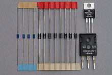
A Schottky diode, also known as a Schottky barrier diode or a hot-carrier diode, is a semiconductor diode developed when a semiconductor and a metal come together. It switches easily and has a low forward voltage drop.
For decades, Schottky diode has been used as the main components in frequency mixer and RF power detector circuits.
In 1938, Walter Schottky, the son of German mathematician Friedrich Schottky, defined how a junction made up of complex metal combinations and a doped semiconductor material would rectify. This thesis resulted in the Schottky diode.
Cat’s-whisker detectors, which were used in the early days of wireless, and metal rectifiers (used in early control applications) are some examples of primitive Schottky diodes.
Index
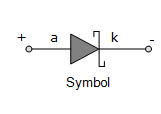
Symbol of Schottky Diode
The symbol for Schottky diode is given as
Construction of Schottky Diode
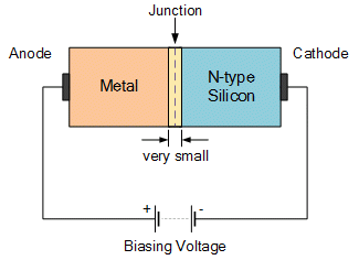
- The Schottky diode junction is created by plating a very pure metal onto a wafer that has been doped with either p-type or n-type dopant atoms, usually by evaporation or sputtering when under vacuum.
- As soon as the materials come into contact their Fermi levels become equal and thermal equilibrium is formed.
- By flowing into the metal, electrons from the semiconductor lower their energy level.
- Charge accumulates at the interface, distorting the semiconductor’s energy bands.
- This produces an energy barrier, known as the Schottky barrier, which prevents the flow of electrons from n-type material into the metal without assistance from an external energy source of the correct polarity to elevate their energy above that of the Schottky barrier height.
- The barrier height is raised by the external energy of the opposite polarity, preventing conduction.
- As metal comes into contact with an n-type semiconductor during chip fabrication, electrons diffuse out of the semiconductor into the metal, leaving an area under the contact known as the “depletion layer” with no free electrons.
- Since each donor atom lost its excess electron, this region contains positively charged donor atoms. This makes the semiconductor positive with respect to the metal.
- Diffusion lasts until the semiconductor becomes so positive in comparison to the metal that no more electrons will enter it.
- The contact potential is the internal voltage difference between the metal and the semiconductor, which is normally between 0.3 and 0.8 V for typical Schottky diodes.
Differences Between P-N Junction and Schottky Diode
| Schottky Diode | P-N Junction Diode |
|---|---|
| Forward current due to thermionic emission. | Forward current due to diffusion currents. |
| Reverse current is only possible because the majority of carriers are able to overcome the barrier. | Reverse current due to minority carriers diffusing to the depletion layer and drifting to the other side. |
| Cut-in voltage is small. | Cut-in voltage is large. |
| High switching speed, because of majority carrier transport. No need for recombination time. | Switching speed limited by the recombination time of the injected minority carriers. |
| As there is no recombination in depletion layer, Ideality factor about 1. | Because of recombination in depletion layer, Ideality factor is about 1.2-2.0. |
Read About Shockley Diode.
V-I Characteristics of Schottky Diode
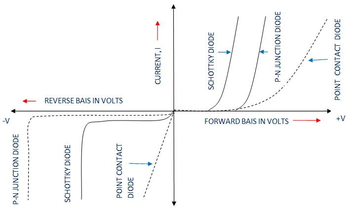
The current flow in the Schottky diode is represented by the vertical line in the diagram below, while the voltage applied across the Schottky diode is represented by the horizontal line.
Schottky diodes have V-I properties that are nearly identical to P-N junction diodes. However, as opposed to a P-N junction diode, the forward voltage drop of a Schottky diode is very mild.
Energy Band Diagram
The energy band diagram for metal and N type semiconductors before contact is
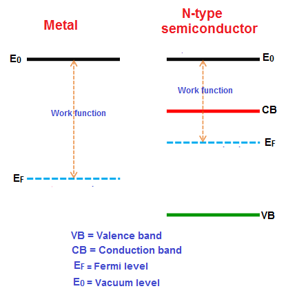
The metal and semiconductor have varying energy levels. On the N-type semiconductor side, the Fermi frequency is higher than on the metal side.
Electrons with a higher energy level have more potential energy than electrons with a lower energy level. As a result, the electrons in an N-type semiconductor have a higher potential energy than those in a metal.
The energy band diagram for metal and N type semiconductors after contact is
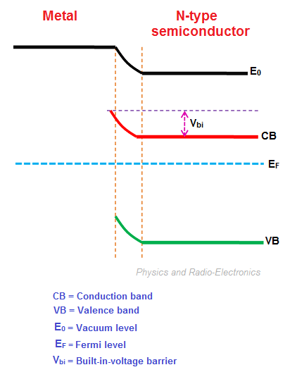
When metal is combined with an n-type semiconductor, a schottky diode is formed. The difference between the work functions of a metal and an n-type semiconductor determines the schottky diode’s built-in voltage.
Current in Schottky Diode
The current in the Schottky diode is because of the electrons (majority carriers) in N-type semiconductor as is given by the equation
\(I_T = I_{\mbox{Diffusion}} + I_{\mbox{Tunneling}} + I_{\mbox{Thermonic}}\)Where,
\(I_{\mbox{Diffusion}}\) is the Diffusion current.
\(I_{\mbox{Tunneling}}\) is the Tunneling current.
\(I_{\mbox{Thermonic}}\) is the current emitted through the electrodes as a result of electron ejection due to thermal energy.
Diffusion Current
This current is the result of concentration gradient and diffusion current density of electrons.
\(I_{\mbox{Diffusion}} = \left( D_n \times q \times \frac{dn}{dx}\right)\)
Where,
\(D_n\) is the diffusion constant of electrons
\(q\) is electron charge
Schottky Diode Drawbacks
Schottky diodes’ most obvious drawbacks are their poor reverse voltage ratings and high reverse leakage current. The reverse voltage of silicon-metal Schottky diodes is usually 50 V or less. There are few higher-voltage models on the market. Since reverse leakage current increases with temperature, it causes thermal instability.
Applications of Schottky Diode
There are several types of Schottky diodes, which are classified mainly by barrier height, which is a property of the doping applied to the semiconductor layer and the metal deposited on it. Schottky diodes come in a variety of configurations and packaging options.
Some of the major applications of Schottky diodes are
1. Charge Controlling
Schottky diodes can be used to precisely load or unload single electrons in semiconductor nanostructures such as quantum wells or quantum dots due to their efficient electric field power.
2. In Solar Cell
Since the power supply is needed around the clock, solar cells are normally connected to rechargeable batteries, most commonly lead-acid batteries. In a relative pattern of solar cells, a diode will be used so solar cells would not accept the applied charge in reverse.
3. In RFmixers
Because of its high switching speed and top frequency capability, the Schottky diode consists of radio frequency functions. Schottky barrier diodes are useful for high-performance diode ring mixers.
4. For voltage Clamping
Schottky diodes have a voltage drop of 0.15 V to 0.46 V at forward biases of about 1 mA, which makes them useful in voltage clamping applications and preventing transistor saturation. This is because of Schottky diode’s higher current density.
Electrowetting
When a Schottky diode is formed with a droplet of liquid metal, such as mercury, in contact with a semiconductor, such as silicon, electrowetting can be observed. The magnitude and sign of the voltage applied to the mercury droplet depends on the doping type and density in the semiconductor. This phenomenon is known as ‘Schottky electrowetting‘.
FAQs
Connect the anode of the Schottky diode to the red positive test lead, and the cathode of the diode to the black common test lead. A “beep” or a “buzz” from the multimeter can be heard.
Schottky diodes are used in high-frequency applications because of their low turn-on voltage, fast recovery time, and low energy loss. Schottky diodes can rectify a current because of these properties, which allow for a fast transition from conducting to blocking states.
Since schottky diodes have a negative temperature coefficient, their Vf decreases as they heat up, you can’t parallel them.
Read More on Diodes