A PIN diode is a diode with a large and undoped intrinsic semiconductor region which is wedged between a p-type and an n-type semiconductor region.
Since they are used for ohmic connections, the p-type and n-type regions are usually highly doped.
In comparison to a standard p–n diode, this diode has a large intrinsic field. Because of its large intrinsic field, the pin diode is a poor rectifier.
Index
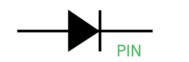
Symbol of PIN Diode
The symbol for a pin diode is
Construction of PIN Diode
As already said, pin diodes have an intrinsic un-doped layer (with high resistivity) wedged between a P-N junction; we will now examine the diode’s construction in detail.
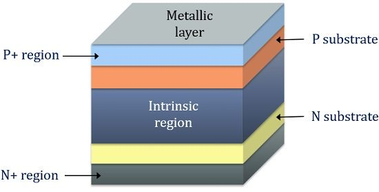
- Pin diodes may be built in two separate structures: Mesa and Planar. Layers that are already doped are grown onto the substrate in a mesa configuration (intrinsic layer).
- The amount of doping and the thickness of the layer can be adjusted to meet the needs of the application.
- An epitaxial layer is grown onto the substrate material in a planar configuration, and the p+ region is formed by ion implantation or diffusion. Similarly, an N+ region is formed on the opposite side of the substrate. The intrinsic region has extremely high resistivity on the order of 0.1-m.
Working of PIN Diode
Although the working of pin diodes are identical to that of a standard diode, there are several variations due to the added intrinsic layer. Pin diodes are poor rectifier, but they are commonly used in switches, attenuators, and other circuits.
Forward Biased Operation
- As the PIN diodes are subjected to forward bias, the depletion area at the p-n junction decreases. As the depletion area is reduced, current begins to pass through the diode.
- In forward bias, the PIN diodes act as a variable resistance.
- A strong electric field is generated around the junction, which accelerates the transport of charge carriers from the P region to the N region.
- As a result of the faster processing, pin diodes are used in high-frequency applications.
Reverse Biased Operation
- When the pin diodes are reverse biassed, the width of the depletion area increases.
- The entire intrinsic layer would be wiped clean of charge carriers at a certain reverse bias voltage.
- This voltage is referred to as the swept-in voltage with a value of -2 volts. It is used for switching purposes in reverse bias
Characteristics of PIN Diode
- The depletion layer becomes fully depleted at a lower level of reverse bias. When the depletion layer is fully depleted, the capacitance of the pin diode becomes independent of the bias level.
- This is due to the intrinsic layer having relatively little net charge. Since the degree of capacitance is usually lower, RF signal leakage is smaller than in other diodes.
- When biassed forward, the diode acts more like a resistor than a nonlinear device, producing no rectification or distortion.
- The resistance is proportional to the bias voltage. Since pin diodes emit less distortions than standard diodes, they are used as RF switches or variable resistors.
Limitations
- Less sensitive.
- Confined area.
- Response time is very low.
Applications of PIN Diode
The following are the main applications of PIN diodes:
- It is used as a high voltage rectifier. The intrinsic layer in the diode acts as a barrier between the two layers, allowing higher reverse voltages to be accepted.
- The PIN diodes are an excellent radio frequency transition. The intrinsic layer between the P and N layers expands the space between them. When the PIN diodes are reverse biassed, this reduces the capacitance between the two zones, increasing the degree of isolation.
- The PIN diodes are used as a photodetector to transform light into current that exists in the depletion layer of a photodiode; expanding the depletion layer by adding the intrinsic layer improves efficiency by increasing the amount in which light shift happens.
- This diode is an ideal element for providing electrical switching in electronic applications. It is primarily used in RF design applications, as well as switching or attenuating elements in RF attenuators and RF switches. The PIN diode will provide much higher degrees of accuracy than RF relays, which are often the only other choice.
FAQs
Yes, for RF and microwave manufacturers, the PIN diode is one of the most flexible models.
A PIN diode works on the principle of high-level injection.
PIN means positive-intrinsic-negative (PIN) and sometimes refers as negative-intrinsic-positive (NIP)
A Video On PIN Diode
Read More on Diodes